DIY Function Generator Project
Working on electronics without a way of generating signals involves a lot of guesswork and dead ends. Since a proper function generator is a bit out of my price range, I set out to try and create my own specifically for audio and RF projects!
On the whole the project was a success, although it is far from perfect and there are quite a few things I’d like to change and implement in a future version before making the CAD files and firmware publicly available. My main reason for writing this is to work through my own thoughts and to share what I’ve done in a way that is (hopefully) useful to someone attempting a similar project. Maybe one or two of my ideas/circuits can be a jumping off point for your own designs :)
Goals
I don’t have a lot of experience using function generators, so I wasn’t exactly sure what features I’d need. Some of the DIY function generators I’ve seen floating around online tend to leave a lot to be desired in terms of their bandwidth and functionality, which actually ended up helping me to figure out what I wanted from my own design
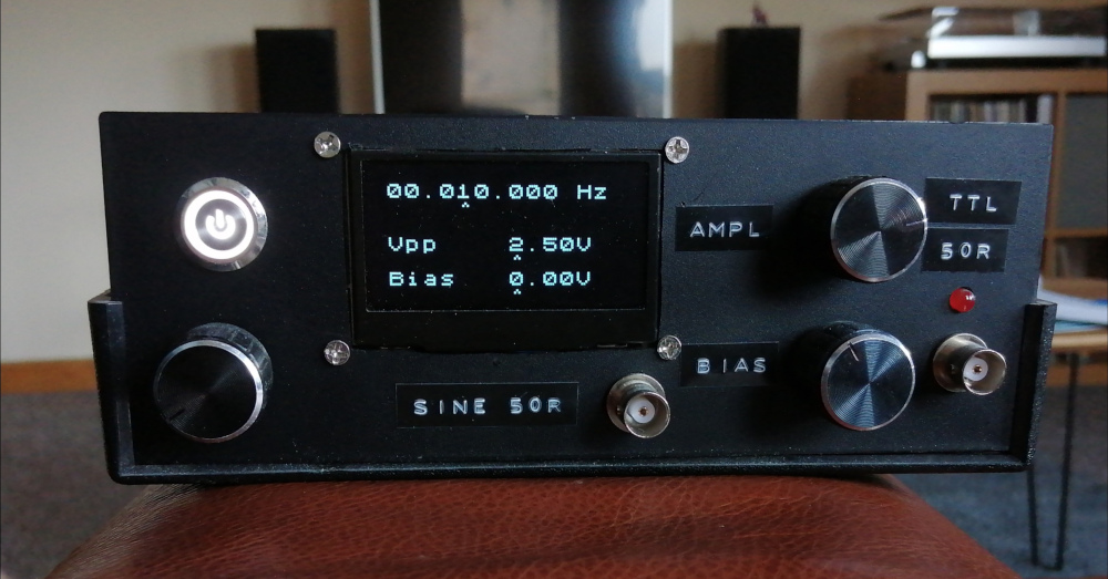
- Digitally controlled variable frequency, amplitude and DC level
- To use an off the shelf DDS module
- +/- 5Vpp output amplitude (terminated)
- 50R output impedance
- 0-5V clock (TTL) output
- Wide bandwidth from AF (~50Hz) to HF (~30MHz)
- -2.5V to 2.5V DC level (terminated)
- Perform basic modulation
- Run off a 15V AC adapter
Analogue Frontend: Sine (Variable)
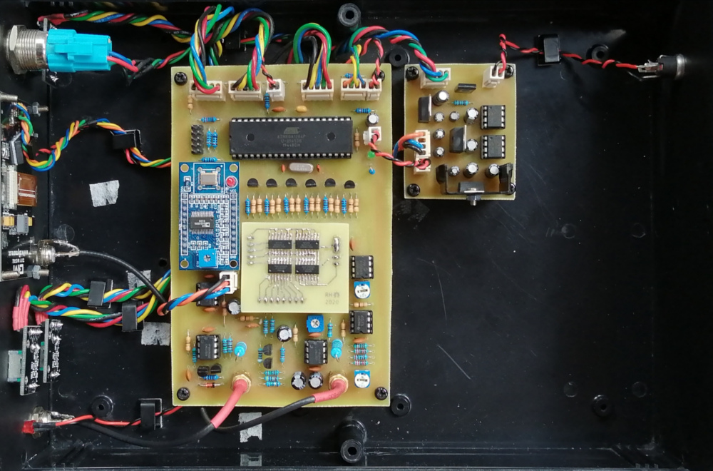
The analogue frontend consists of a DDS module from eBay (AD9850) connected to a digitally controlled attenuator feeding a wideband fixed-gain amplifier
The main requirements of the amplifier were to have a flat passband between 50Hz and 30MHz; and have a gain of roughly 24.4dB (to amplify the ~600mVpp output of the AD9850 to the desired 10Vpp)
An LM6172 dual opamp was selected to be the basis for amplification and buffering. It is also used in the TTL/CMOS frontend hence the bandwidth being a bit overkill - I go by the rule of thumb that says when handling square waves the bandwidth of the device should be at least 3 times greater than the fundemental frequency of the waveform. Its slew rate is also ideal for working with 10Vpp high frequency waveforms
To achieve the desired gain using a single LM6172 would mean reducing the effective bandwidth of the amplifier (due to its gain-bandwidth product) quite considerably. Since it’s a relatively expensive device I decided to split the amplifier into two sections - a cascode common-emitter amplifier using 2N3904 BJTs and an inverting opamp amplifier
Theoretically the gain of the cascode amplifier is around 16dB with a -3dB bandwidth of 50Hz to 35MHz. The emitter bypass capacitors effectively set the lower cutoff frequency (although the overall gain of the amplifier is always limited by their effective series resistance, roughly 4R). The upper cutoff frequency is largely a function of the gain-bandwidth product (transition frequency) of the transistors - the cascode configuration limits the attenuation at high frequency due to the Miller effect. The value of the termination resistor (R23) was figured out by experimentation as a happy medium between the flatness of the passband and gain. Likewise some other component values in the circuit were tweaked after some experimentation
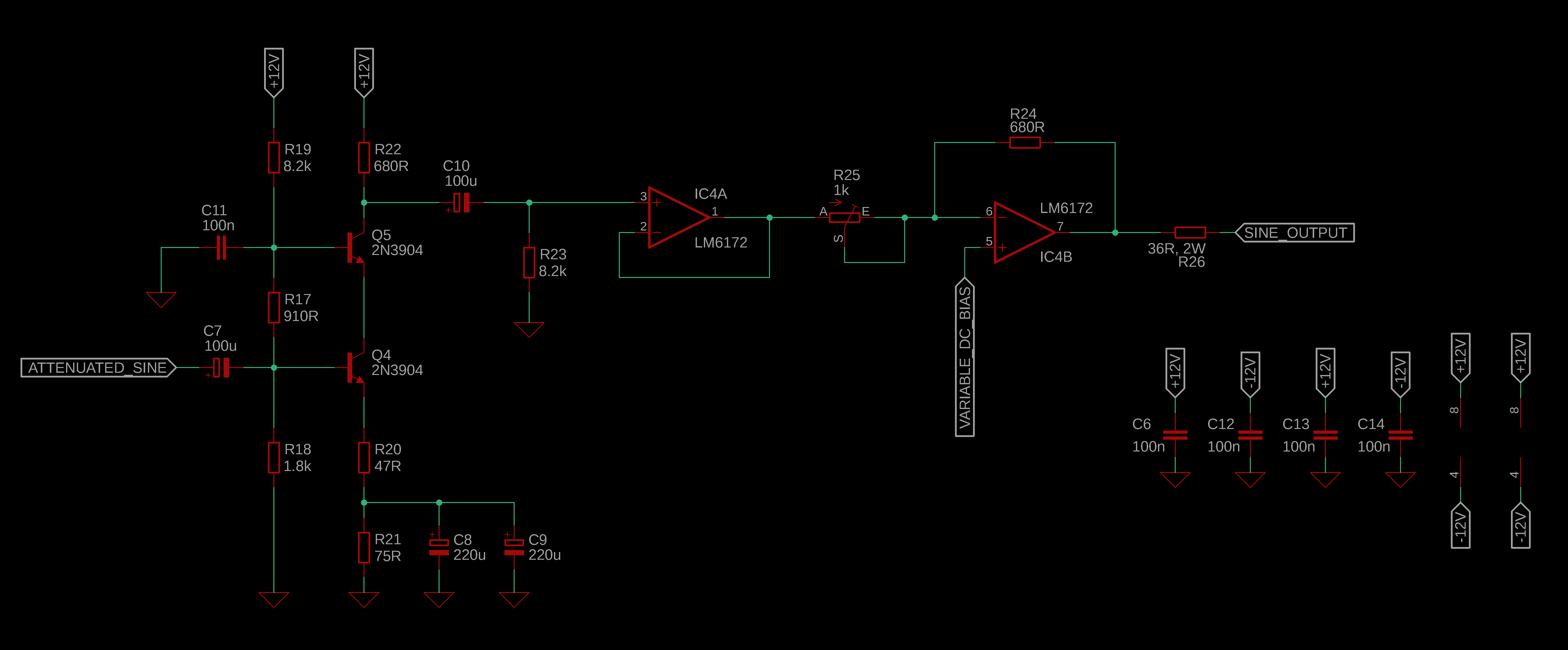
The values of R25 and R24 in the opamp amplifier were also selected to reduce Miller effect attenuation, as advised by the opamp’s datasheet. Their ratio was set in order to make up the rest of the required gain (8.4dB)
The trim pot (R25) allows the amplifier’s gain to be varied for use in certain circumstances, i.e. reducing the gain to allow for finer amplitude adjustments using the same attenuator. The user interface could then be altered in the firmware to reflect this. It also may be used to account for any insertion loss introduced by the attenuator
According to its datasheet the LM6172 has an output impedance of 14R, so a 36R resistor was added to the output to bring the overall output impedance up to 50R. I used a 2W resistor in case of the event of a short circuit (50R * (10V / 50R)^2 = 2W) - although the opamp has built-in short circuit protection so the output current wouldn’t actually reach this level. Better safe than sorry!
Variable DC Source
To create a digitally controlled bipolar voltage source, I used a low-cost 12-bit DAC and an opamp. The only requirement was an output voltage range of +/- 5V
I selected a MCP4821 since it’s cheap, widely available and has a decent datasheet with an example of how to use it as a bipolar voltage source. In the end I used the example from the datasheet along with a design note from Texas Instruments to come up with a suitable circuit
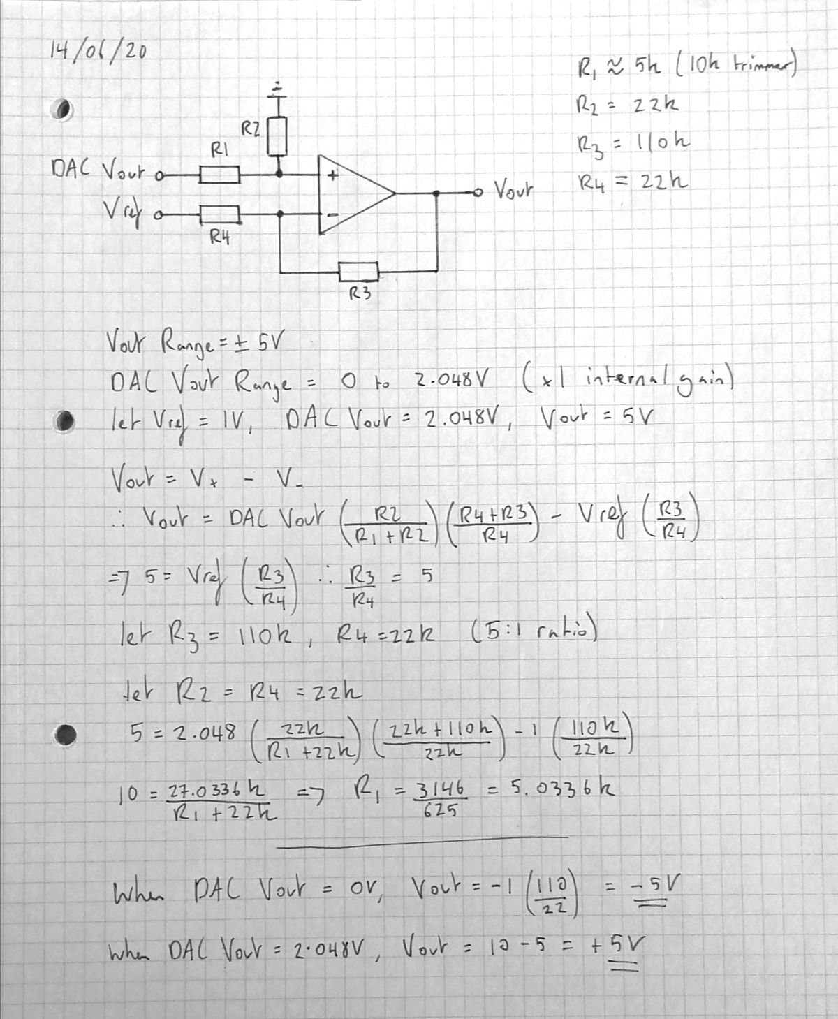
The opamp is setup in a differential amplifier configuration. The output is the difference in voltage between the output of the DAC and the fixed reference voltage (Vref), multiplied by some gain. This allows the output of the DAC to be scaled to the required Vout range. The minimum step size is roughly 2.5mV (10V / 2^12)
I chose to set Vref to 1V to make the maths a bit simpler. In the final circuit Vref is created by a voltage divider with a trim pot. I also added a buffer to the output since I had a dual opamp IC - this probably doesn’t do anything useful since the output is fed into the (high impedance) input of another opamp
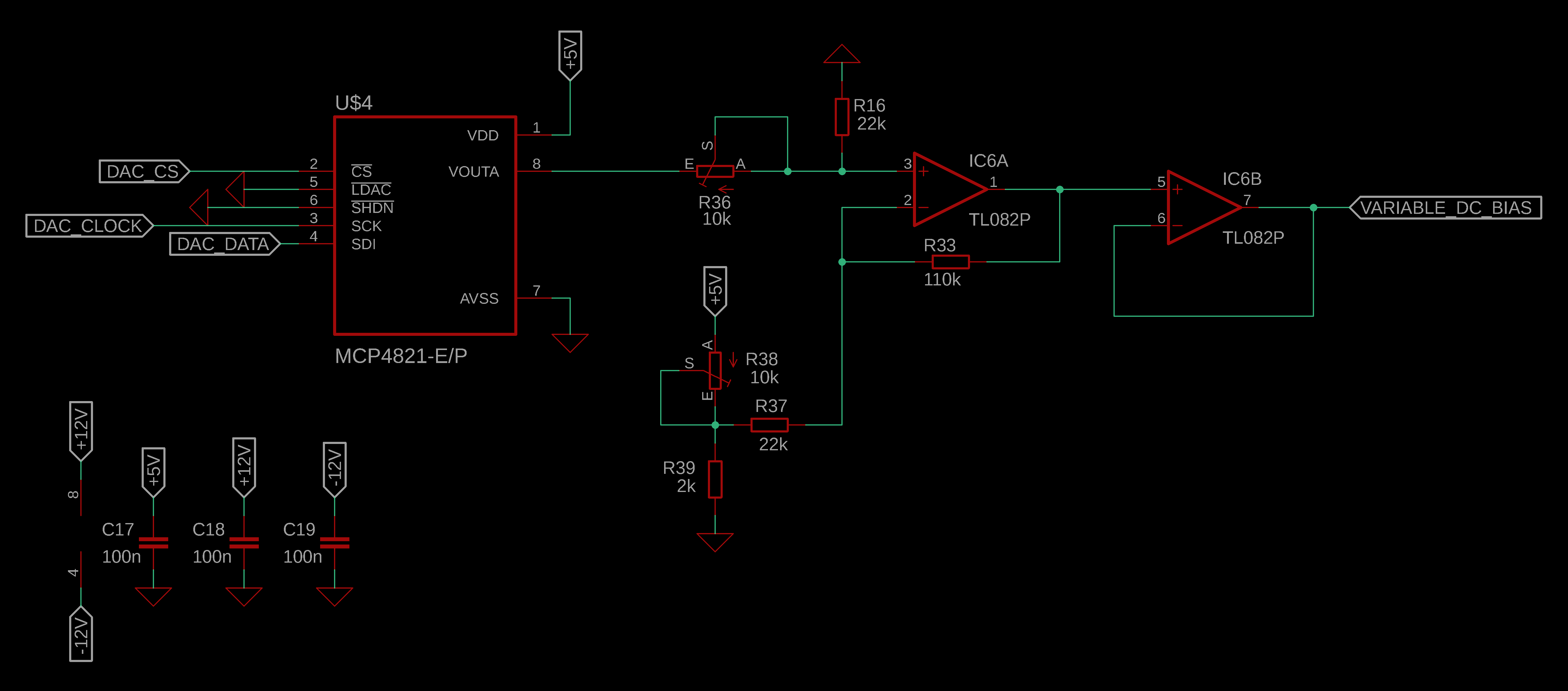
Due to using trimpots instead of low tolerance resistors, the circuit has to be calibrated as follows:
Set the DAC word to 0 (-5V)
Adjust R38 until Vref = 1V
Set the DAC word to 2048 (0V)
Adjust R36 until Vout = 0
In the firmware, to get a particular output voltage the data word that corresponds to the desired value is calculated according to a linear equation:
int calculateBiasWord(float dcBias) {
  float slope = (4095 - 0) / (dcBiasMax - dcBiasMin); // (y2 - y1) / (x2 - x1)
  float yIntercept = 4095 - (slope * dcBiasMax); // y2 - (m * x2)
  int biasWord = (slope * dcBias) + yIntercept; // mx + c
  return biasWord;
}
This assumes that the DAC and the differential amplifier are perfectly linear, so it’s not an ideal solution but it’s good enough. The accuracy could be increased slightly by entering the actual (measured) max and min values of Vout after calibration
Attenuator
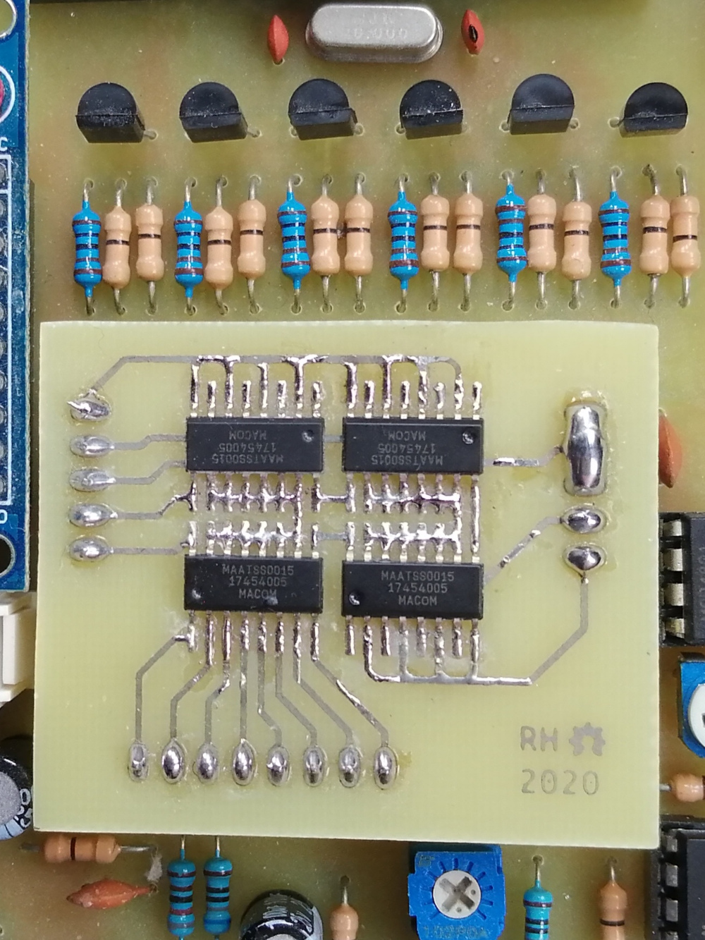
The digitally controlled attenuator was made using 4-bit 15dB MAATSS0015 attenuator chips. I used four of these attenuator chips in series to give 6-bits of control and a maximum attenuation of up to 60dB. Since I can only etch single-sided circuit boards I decided to construct the attenuator on a daughter board that plugs into the main PCB
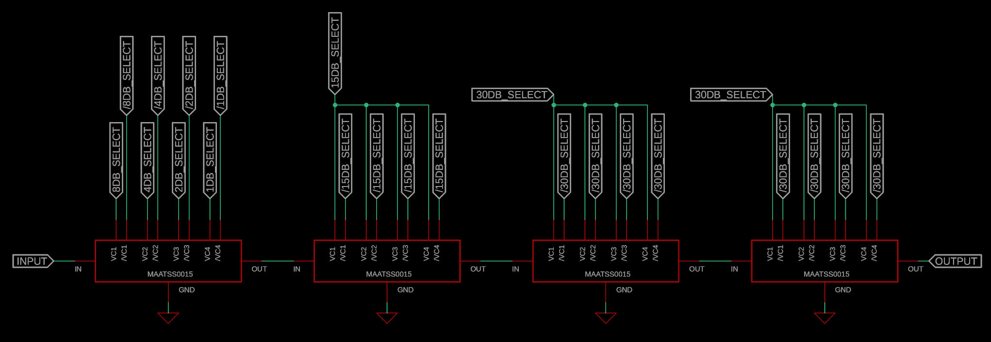
Confusingly, it has both an active high and an active low input for each bit. I didn’t know how to interpret this so I made an array of not gates using 2N7000 MOSFETs to connect to the active low inputs. In the end the traces to the active low inputs were cut since it only operates correctly if either the active high or active low inputs are in use
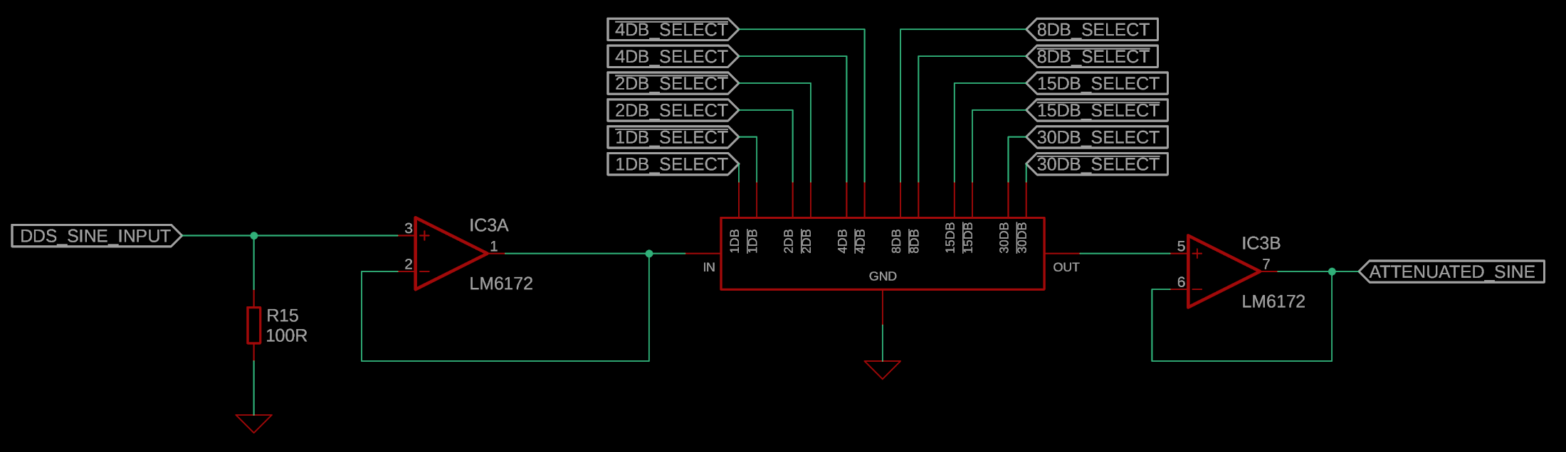
An LM6172 is used to buffer the input and output of the attenuator. The output of the DDS module is terminated with a 100R resistor - I found this to be the optimum value for maximum amplitude and bandwidth
Analogue Frontend: TTL/CMOS (Fixed)
The AD9850 outputs both a sine and a square wave, so I thought I may as well include it as an additional output. The square wave it generates becomes fairly distorted by about 3MHz so I elected to use it to drive a Scmitt trigger circuit to derive a nice, clean output from it
I took the design of the Scmitt trigger from an EEVBlog forum post which I now can’t find. I attempted to design my own but I couldn’t make it stable for the life of me. Understanding how to analyse circuits involving hysteresis is a bit beyond my skill level. All credit goes to the original creator!
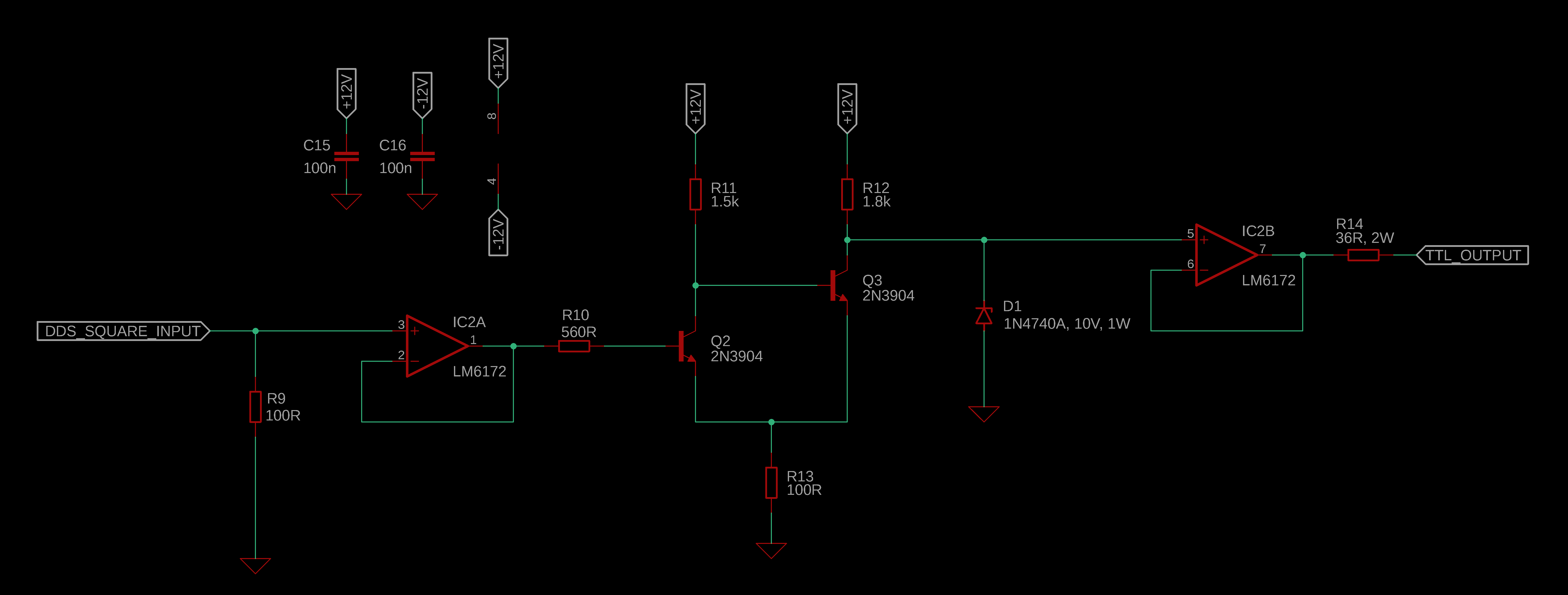
I added the buffers and a 10V zener diode on the output of the Scmitt trigger in an attempt to limit overshoot. The output resistor (R14) is there for to make up the 50R output impedance as described earlier
In practise the signal is only really usable up to 10MHz. For a future revision I think I’d need to go back and try to properly understand the operation of the circuit to increase its performance
Power Supply
The analogue circuitry was designed with +12V and -12V power rails in mind. A +5V rail was also required for the digital circuitry. The negative rail was the main area of concern when designing the power supply since the positive rails could be easily generated with linear voltage regulators
For the -12V rail the worst case scenario would be if the output was short circuit with the output amplitude at 10Vpp with -5V DC level. The negative rail would theoretically have to deliver up to 200mA (10V / 50R). In reality the opamp used in analogue frontend has short circuit protection so the current requirements wouldn’t be as demanding. When terminated properly the peak current requirement would be 100mA (10V / 100R)
I decided to split the difference and say that the negative rail needs to be capable of delivering up to 150mA. I nominally chose 1A to be the current required for the +12V and +5V rails combined
The current requirements of the negative rail were low enough that I elected to use charge pumps. The TC962 seemed suitable for the task. Two devices together in parallel should theoretically deliver 160mA of current
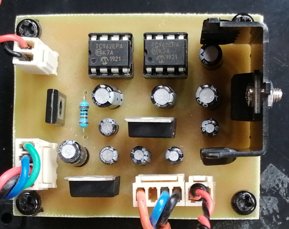
I’ve managed to lose the CAD files so I can’t show a schematic, but it’s fairly a straight forward circuit
A +12V and a +5V regulator are connected to the +15V line from the AC adapter. It should be noted that the +5V regulator is quite inefficient being driven from this voltage and runs hot, hence the heatsink
The charge pumps are connected as per the example in the datasheet. Their input is fed by the +15V line. An active low pass filter (capacitance multiplier) is connected to the output and then into a -12V regulator. The filter helps knock out any switching noise from appearing on the regulated -12V rail
There are sockets on the PCB to connect to the input power supply and an illuminated power switch on the front panel
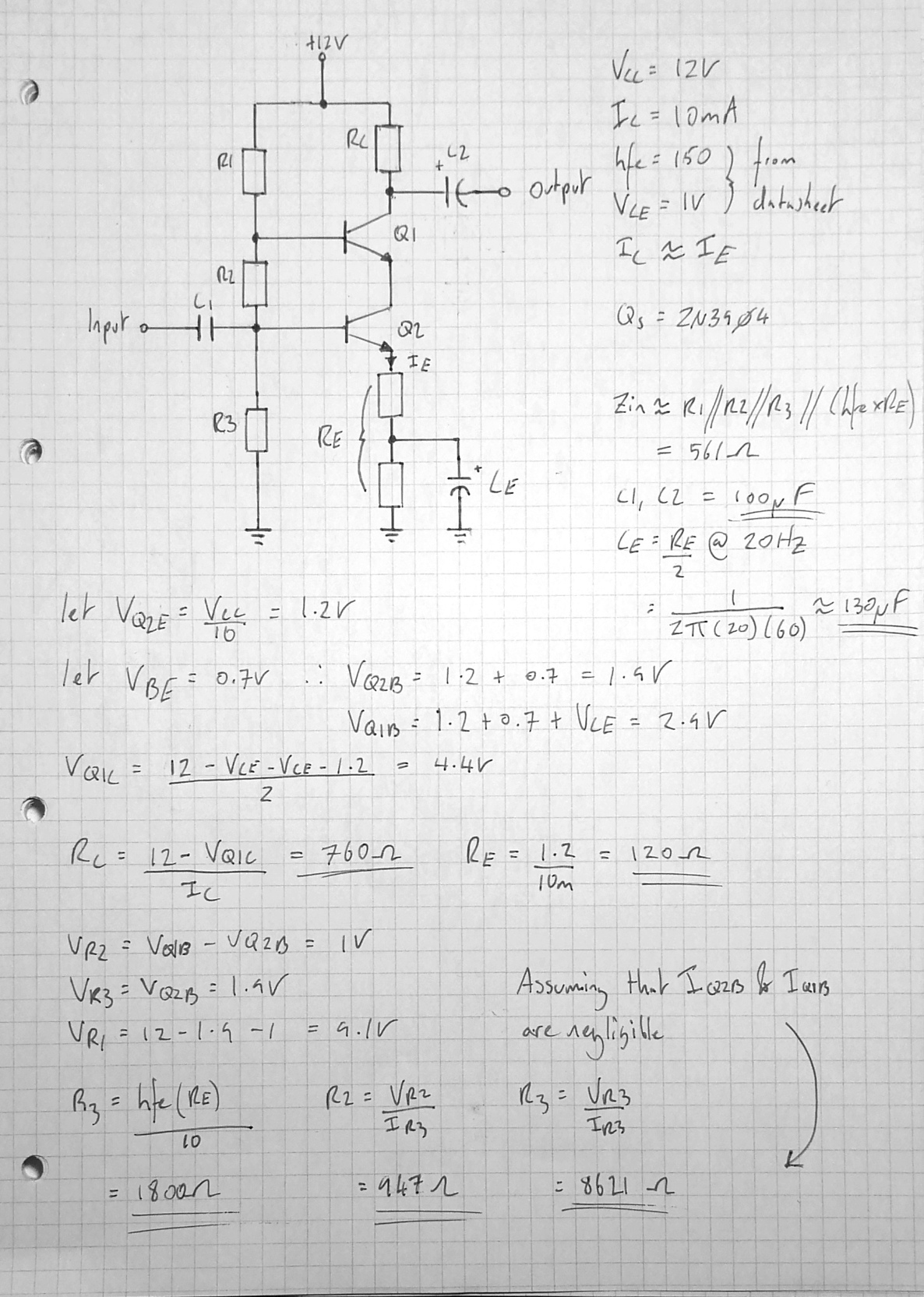
Digital Section (microcontroller)
I used an Atemga1248P microcontroller due to the number of I/O pins I was planning to use and the amount of memory it has (4k RAM, 128k flash). It’s connected as per the datasheet with a clock speed of 20MHz. I also added a programming header for use with a USBasp programmer
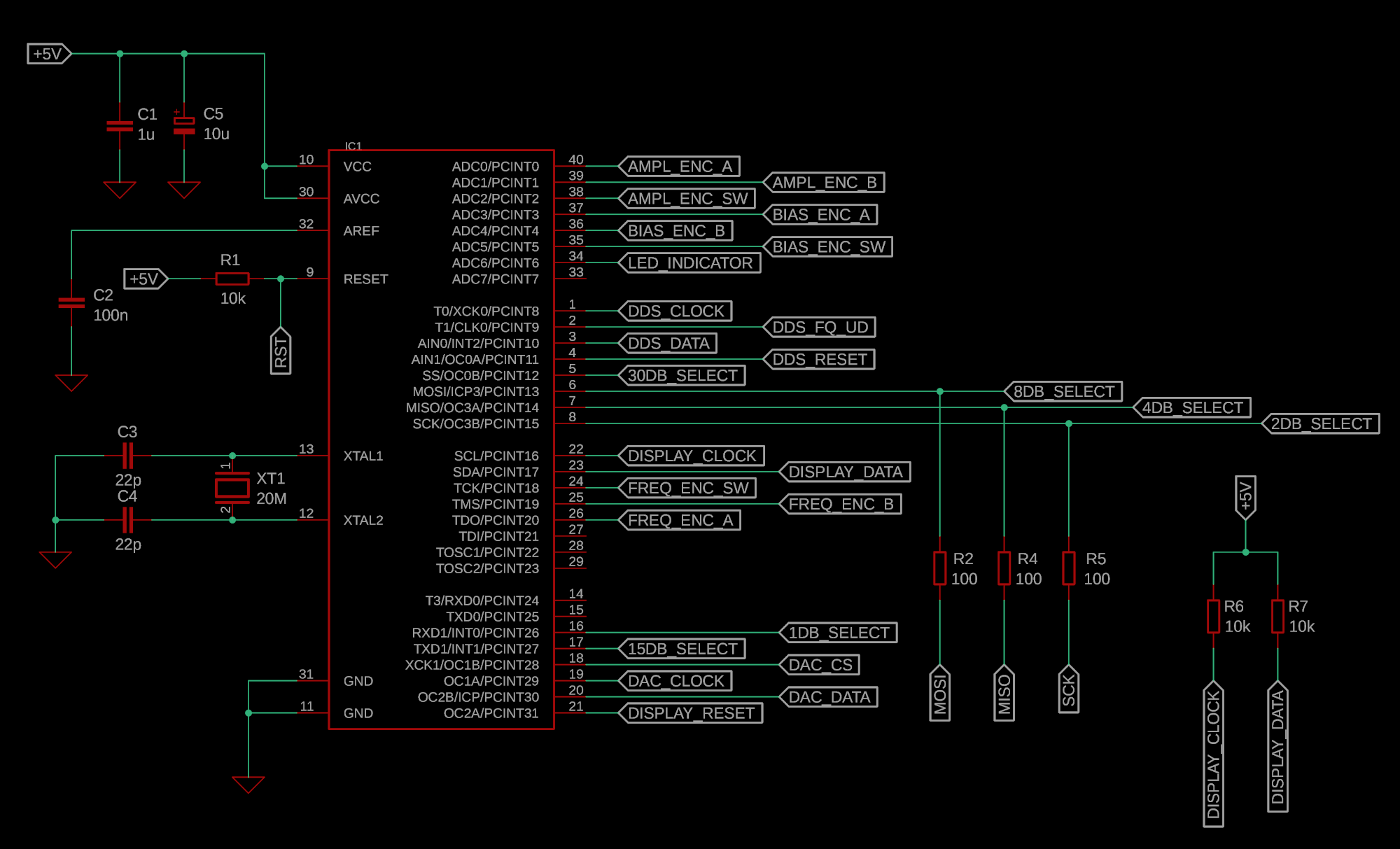
The user interface uses a white-on-black OLED display and three rotary encoders to control frequency, amplitude and DC level
Unfortunately I was unable to implement any modulation in firmware, although I do think it is possible with this design. My understanding of the maths just isn’t quite there yet
Improvements
Although I didn’t manage to get the function generator to produce any modulated functions, it works well for generating sine waves up to 20MHz and square waves up to 10MHz
In a future revision there’s a few improvements I would want to explore:
Using a proper DDS or some other method of signal generation - it doesn’t matter how good the rest of the design is the output signal can only be as good as its source. The sine wave becomes quite distorted at around 15MHz although a lot of the higher harmonics are filtered out by the time the signal reaches the output…
Simplifying the user interface down to using only one rotary encoder and maybe some buttons would make it easier to use and the firmware more responsive - polling 3 rotary encoders is really not efficient!
A better power supply design would help reduce noise and increase its efficiency. Using a smaller, less noisy display would also help this; a switching power supply is used to generate a negative voltage to drive the OLED. At high output levels some noise does unfortunately find its way into the signal
Narrowing the overall spec of the function generator could potentially make the design focused on fewer performance characteristics. For example, a function generator just for RF use would have smaller amplitude requirements and could use transformer coupling since low frequency response wouldn’t matter as much